The world’s fastest supercomputer is American again. President Donald Trump’s dedication to #MAGA (Making America Great Again) is showing results big time. Chief among them are the Tax Cut and Jobs Act (2017-2018), a booming economy and a growing stock market.
But economic prosperity also needs military might and IT technology that’s worthy of a superpower.
During the sad 8 years of the Obama presidency, the U.S. has ceded the #1 and #2 titles in the TOP500 super computers list to China.
That’s over.
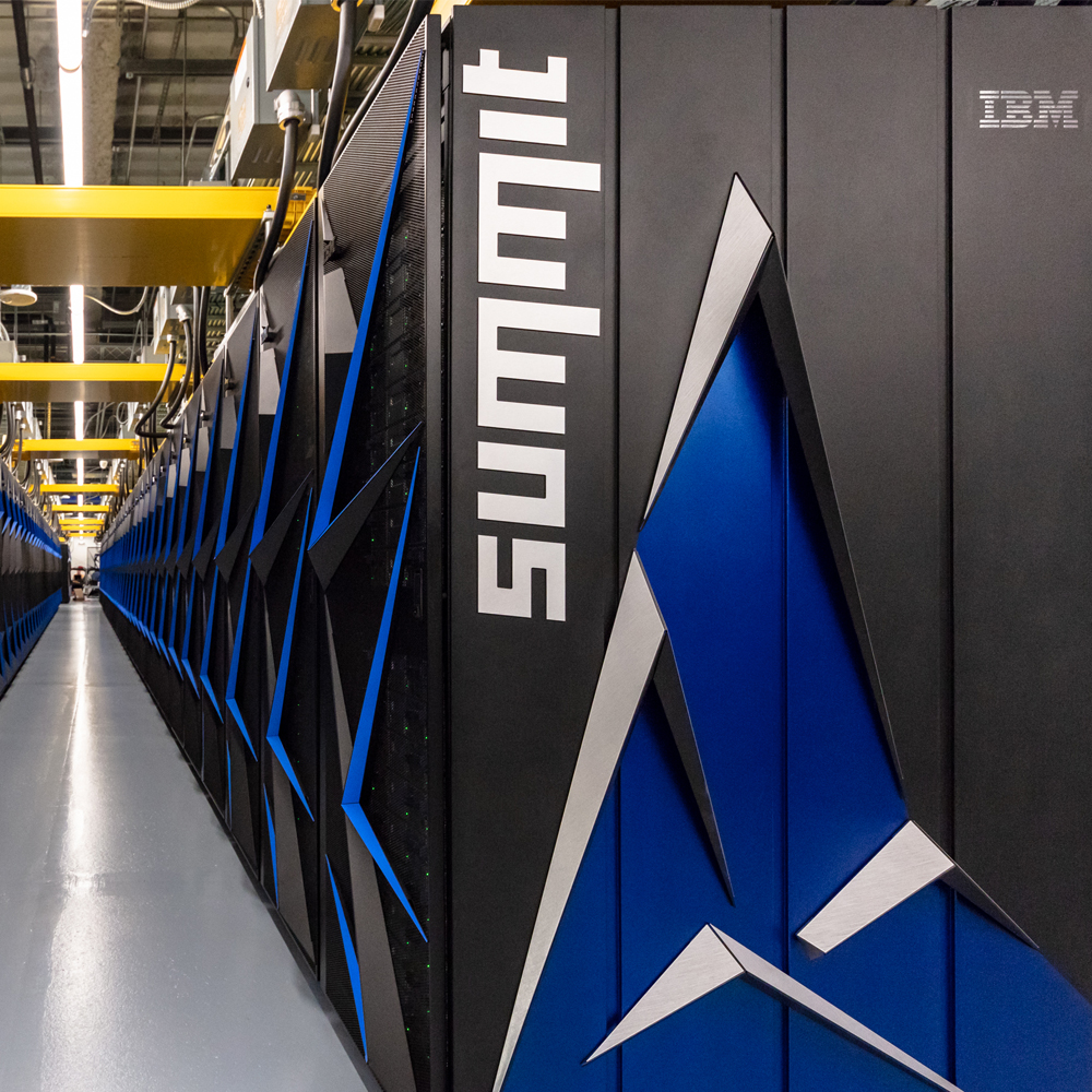
Summit: the new American #1
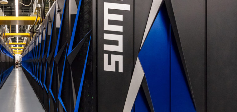
The new #1 is made in America: Summit. The U.S. Department of Energy tasked IBM to build it for the Oak Ridge National Laboratory.
Summit is not just about more and faster chips. For starters, it runs on Red Hat Enterprise Linux (RHEL), finally putting CentOS with its outdated everything to rest.
With 200 Petaflops, it literally blows through the charts. It’s one bold statement: Summit is 215% (in words: two hundred and fifteen percent) faster than China’s Sunway TaihuLight (a “mere” 93 Petaflops). Let that sink in for a moment!
As the fastest of all supercomputers, Summit is very different from the average HyperScale Data Center. Summit not only excels at typical supercomputing jobs, it also boldly goes where most traditional super computers won’t go: Artificial Intelligence (AI) and Machine Learning (ML).
The design of Summit features an impressive hybrid architecture and some of the best technology the US has to offer. IBM, Nvidia, and Mellanox worked on the hardware. Red Hat contributed Red Hat Enterprise Linux as the software. Every node contains two IBM POWER9 processors and six NVIDIA Volta v100 GPUs.
NVIDIA’s V100 GPUs with 7.8 TFLOPS/s
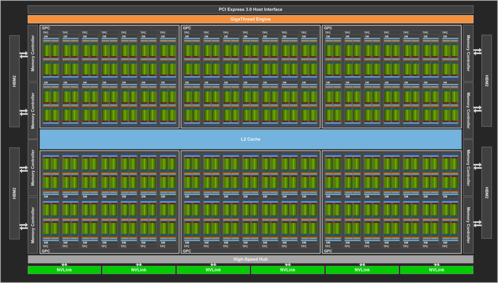
The NVIDIA Tesla V100 accelerator has a peak performance of 7.8 TFLOP/s (double-precision) and is responsible for the greatest part of computational breakthrough performance on the Summit. Each V100 is home to 80 streaming multiprocessors (SMs), 16 GB of high-bandwidth memory (HBM2), and a 6 MB L2 cache that is available to the SMs.
Besides, the GigaThread Engine is in charge of distributing the computional jobs among the SMs and eight 512-bit memory controllers supervise the access to the 16 GB of HBM2 memory. To push the competitive edge even further the V100 rely on NVIDIA’s NVLink interconnect to move data between GPUs also from CPU-to-GPU:
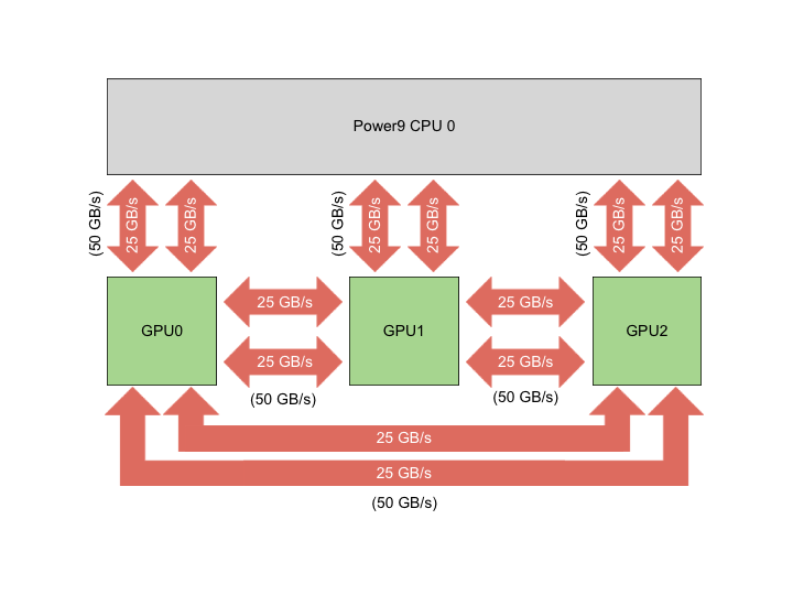
The NVIDIA’s high-speed NVLink, which sports a 50 GB/s bi-directional data transfer rate, so the maximum speed per second can be up to 100 GB/s.
NVIDIA’s V100 SMs
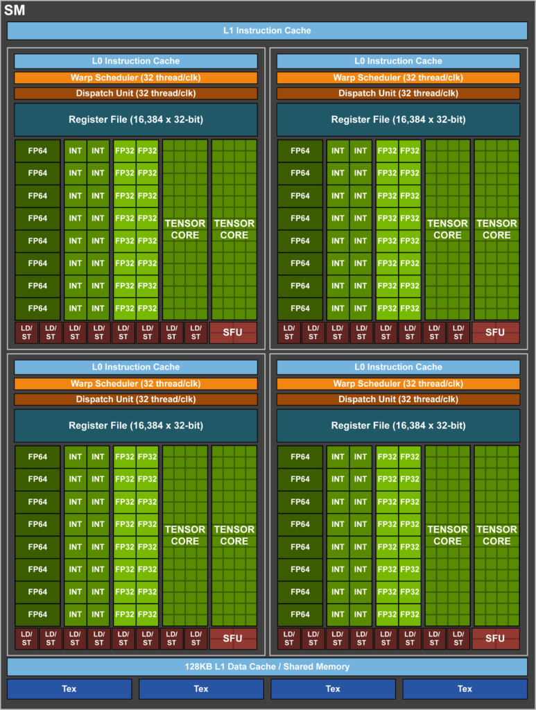
Every V100 is home to 80 streaming multiprocessors (SMs). To understand how the Summit taps into so much computational power you need to literally drill down into the SMs and see what’s in there.
Every SM of the NVIDIA V100s holds 32 FP64 (double-precision) cores, 64 FP32 (single-precision) cores, 64 INT32 cores, and even 8 very special tensor cores. On top of it, there is also a 128-KB combined memory block for shared memory and a L1 cache, which can be configured to allow up to 96 KB of shared memory. Furthermore, every SM sports four texture units, which take advantage of the L1 cache. Now that’s a mouthful.
HBM2 with 900 GB/s
Next up in Summit’s impressive hybrid hardware architecture is the HBM2. HBM2 is short for high-bandwidth memory.
Let’s recap that: Every NVIDIA V100 offers access to 16 GB of high-bandwidth memory, but the real kicker is the access speed of up to 900 GB/s. In charge of supervising and coordinating the access to this memory are eight 512-bit memory controllers. In order to smooth the ride, all accesses to the HBM2 are performed via a 6 MB L2 Cache.
Tensor Cores
The Tesla V100 is home to 640 tensor cores. Since there are 8 per SM, we get to 8 x 80, which translates into a total of 640 tensor cores. What is a tensor? Actually, a tensor means just a generalized matrix. It can be a 1-dimensional matrix. That would be plain and simple a vector. Or a 3-dimensional matrix. Think about a Rubik’s Cube. While a Rubik’s Cube is absolutely symmetrical with a 3 x 3 x 3 structure, the tensor cores of NVIDIA’s V100 are slightly different. Imagine a 4 x 4 matrix, which is actually just a 2-dimensional grid of numbers and which, in this example, we call Matrix D.
The Matrix D is the result of the product of (Matrix A x Matrix B) + Matrix C. The numbers in these matrices are FP16 or FP32. FP stands for Floating Point and means a real number which requires 16 bit. That’s why it’s called FP16 for short or also “half precision”. Usually “full precision” means 32 or 64 bit.
That’s maybe hard to imagine. I hear you, you get a picture. A picture says more than thousand words.
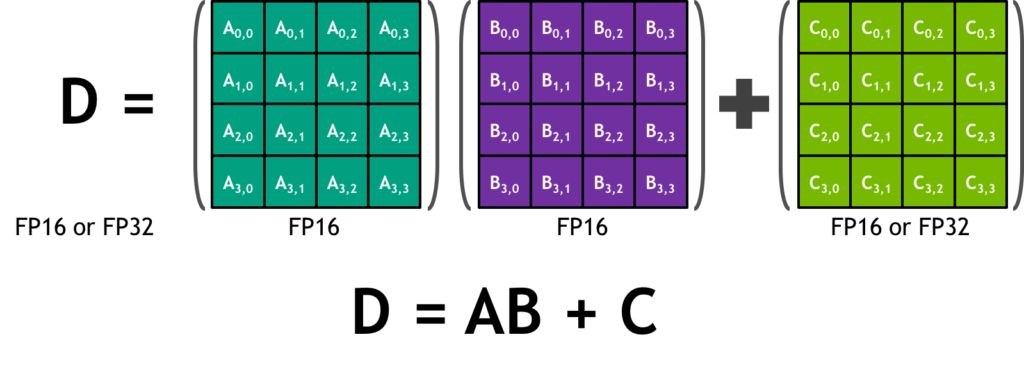
Four times four elements yields 16 elements. Every one of these 16 elements results from the A x B matrix multiplication. Without going into further details, this is the content of just one tensor core in the NVIDIA Tesla V100. Now picture 640 tensor cores at the same time. Wow, that’s very impressive. Even handling all these floating point values is already an amazing feat all by itself.
The NVIDIA V100 in the Summit goes even further as it sports unified memory.
Unified Memory, Nodes, and more
In order to simplify programming for the the NVIDIA Tesla V100s in the Summit, IBM gave it a unified memory architecture. The IBM Summit is well equipped with memory:
- Memory/node: 512GB DDR4 + HBM,
- NV Memory/node: 1600GB,
- Total System Memory: >10PB DDR4 + HBM + Non-volatile.
Every node delivers in excess of 40 TF and the IBM Summit sports about 4,600 nodes. The total performance is an impressive 200 PetaFlop.
Leave a Reply